Homework
assignments for ECE 614 Advanced Analog IC Design, Fall 2011
Homework
guidelines are found here.
Note
that an A in front of the problem indicates an additional problem
from the book’s webpage,
not a problem from the book’s end-of-chapter problems.
Project2
– due Thursday, December 15, design a 12-bit pipelined ADC using 1.5
bits/stage
and capacitor error averaging. Use the ideal op-amp circuit/symbol from
Ch. 30
(see, for example, Fig. 30.34). Some additional comments and
requirements:
1)
Your
design should use the
same symbol footprint as the ideal 12-bit ADC in the Chap30_LTspice
directory
at CMOSedu.com. Also, use the ideal 12-bit DAC from this directory to
help with
your simulations.
2)
Assume
the ADC’s input is
single-ended (it has to be to match the ideal 12-bit ADC’s symbol) so
that the
input of the ADC is a single-ended to differential S/H (Fig. 30.34).
Verify, in
your report, that the op-amp’s input CM voltage doesn’t vary.
3)
Simulations
should show
your ADC along with the ideal 12-bit DAC so that the top level
simulations
contain two symbols, your ADC and the ideal DAC, along with VDD = 1 V
and a,
for example, 100 MHz clock signal.
4)
Use
ideal logic in your
design for clock generation and for the logic that combines the outputs
of the
pipelined stages. It’s okay to use the built-in LTspice digital gates.
5)
Show,
using simulations,
the tolerance of your design to capacitor mismatch and
op-amp/comparator
offset. Show that the performance of (matching in) the earlier
pipelined stages
is more critical than the later stages.
A
PDF report detailing the operation and performance of the design along
with a
zipped up file containing simulations (no raw files) should be emailed
to the
instructor before class time on December 6.
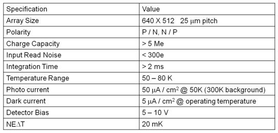
Project1
– due Thursday, October 13, this project has to do with the design of a
readout
integrated circuit (ROIC) for use with a corrugated quantum well
infrared
photodetector (C-QWIP). The C-QWIP is an imager
that operates at lower
temperatures, around 50K, (paper)
useful for infrared sensing (viewing the temperature of objects). The
focal
plane array (FPA) of C-QWIP devices will be bumped to the top of a CMOS
chip
containing your ROIC design. The FPA is connected through “bump pads”
(smaller
than regular bonding pads) on the top of the CMOS chip. A thermal
electric
cooler is used to cool both the C-QWIP FPA and the CMOS chip. Your ROIC
must
fit within a 25 um square layout area (the size of the C-QWIP device,
see the
Table below) and be as low power as possible since there will be
327,680 ROICs
on the chip. Basic requirements are seen in the table below. Some
example
calculations are shown next to the table.
 Example
calculations:
Example
calculations:
For
a 25 um pitch, Iphoto
= 312.5 pA
For
a 25 um pitch, Idark
= 31.25 pA
Using
a 3.3V CTIA (capacitive feedback transimpedance
amplifier) output swing, with a 2 ms integration time, for the maximum
input
photo current:
Iphoto =
(50 mA/cm2)(25 um x 25 um) =
312.5 pA
Iphoto =
312.5 pA = C (DV/Dt)
= C (3.3 V/2 ms) = C (1.65 x 10³ V / s)
C =
312.5 pA/(1.65 x 103
V) = 189 fF
Read
noise = sqrt (kT/C) = 71.4e RMS @ 50K
Swing
due to dark current 330 mV
Design
the ROIC using On’s C5 process (SPICE
models are in C5_models.txt).
One side of the C-QWIP device is
connected to the input of your ROIC circuit. The other side is common
to all
C-QWIPs in the FPA and tied to a common bias voltage.
Requirements:
1)
the
input of your ROIC
must be short-circuit protected so that if a single C-QWIP device
shorts to the
common bias voltage the ROIC is unharmed and doesn’t draw significant
current
2)
the
bias voltage of the
common C-QWIP device can range from 0 to 5 V (not the 5 to 10 seen in
the
table)
3)
the
input voltage of the
ROIC is nominally 2.5 V (so that the voltage across the C-QWIP device
can vary
between -2.5 and +2.5 V)
4)
the
input voltage of the
ROIC stays at nominally 2.5 V during the integration time to avoid
de-biasing
the C-QWIP device (unless the ROIC’s output saturates at the power
supply rail)
5)
besides
the bump to the
C-QWIP device the inputs of your ROIC are row_reset and row_select
6)
the
output of your ROIC is
row-line selectable (with the row_select signal) and
connected to a column line
7)
the
output of your circuit
is an analog voltage corresponding to the integrated current from the
C-QWIP
device
Use
LTspice to verify your hand calculations. Do not layout the ROIC;
however, do
estimate the ROICs layout size. A PDF report detailing the design
considerations, design decisions (including a discussion of the type of
feedback amplifier used and why), and a noise analysis (with
simulations verifying
hand calculations) along with a zipped up file containing simulation
schematics
should be emailed to the instructor before class time on Oct. 13
HW#15
– due Tuesday, December 6, A30.8 and A30.12, check end-of-chapter
online
solutions: JB – 30.25, AL – 30.24, RL – 30.23, BM – 30.22, AT – 30.21
HW#14
– due Tuesday, November 29, A30.9 and A30.11, check end-of-chapter
online
solutions: JB – 30.16, AL – 30.17, RL – 30.18, BM – 30.19, AT – 30.20
HW#13
– due Thursday, November 17, A30.5-A30.7, check end-of-chapter online
solutions: JB – 30.11, AL – 30.12, RL – 30.13, BM – 30.14, AT – 30.15
HW#12
– due Tuesday, November 15, A30.1-A30.3, check end-of-chapter online
solutions:
JB – 30.10, AL – 30.9, RL – 30.8, BM – 30.7, AT – 30.6
HW#11
– due Thursday, November 10, only check end-of-chapter online
solutions: JB –
30.5, AL – 30.4, RL – 30.3, BM – 30.2, AT – 30.1
HW#10
– due Tuesday, November 1, A29.4 and A29.7
HW#9
– due Thursday, October 27, A29.1-A29.3
HW#8
– due Tuesday, October 4, A8.13 and A8.16
HW#7
– due Thursday, September 29, A8.4-A8.10, A21.31, and A21.32
HW#6
– due Thursday, September 22, A8.1-A8.3, and generate the PSD of the
MOSFET’s
drain current for both devices in Table 9.2
HW#5
– due Thursday, September 15, A31.12-A31.14, and check end-of-chapter
online
solutions: JB: 31.21-31.23, AL – 31.24-31.26, RL – 31.27-31.29, BM –
31.30-31.32, and AT – 31.33-31.35
HW#4
– due Tuesday, September 13, A31.8-A31.11, and check end-of-chapter
online
solutions: JB – 31.11 and 31.16, AL – 31.12 and 31.17, RL – 31.13 and
31.18, BM
– 31.14 and 31.19, AT – 31.15 and 31.20
HW#3
– due Tuesday, September 6, A31.6 and A31.7
HW#2
– due Thursday, September 1, A31.2-A31.5, and check end-of-chapter
online
solutions: JB – 31.10, AL – 31.9, RL – 31.8, BM – 31.7, AT – 31.6
HW#1
– due Tuesday, August 30, A31.1 and check end-of-chapter online
solutions: JB –
31.1, AL – 31.2, RL – 31.3, BM – 31.4, AT – 31.5